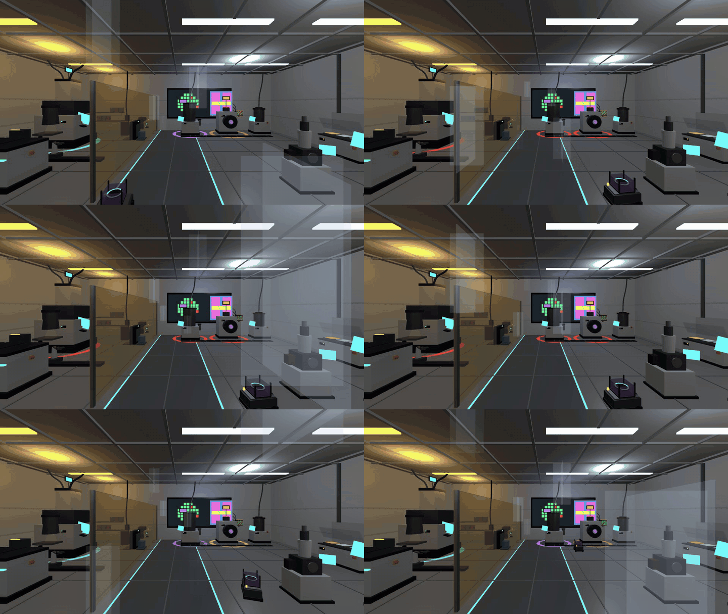
A cleanroom carved into undercity bedrock, running three fab lines whose customers are all in town: a sky130 inference ASIC for the compute center, a 65 nm SPAD readout chip for the sensor network, and double-angle Josephson junctions for the quantum center. One hero wafer walks the whole flow every 104 seconds — and every light that touches it is phase-locked to a number in the ledger below.
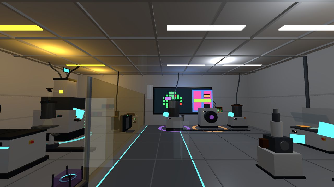
A yellow-bay / white-bay cleanroom under HEPA laminar downflow, sited in bedrock where dust storms and vibration cannot reach a litho stage.
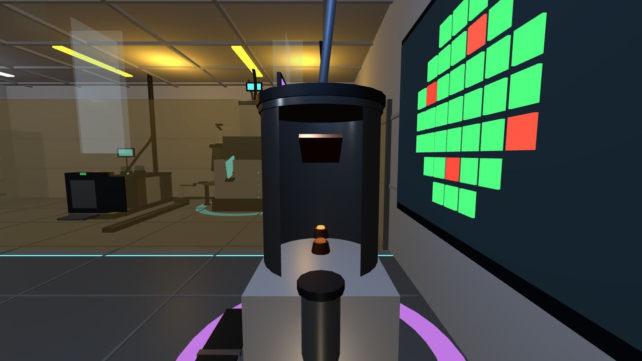
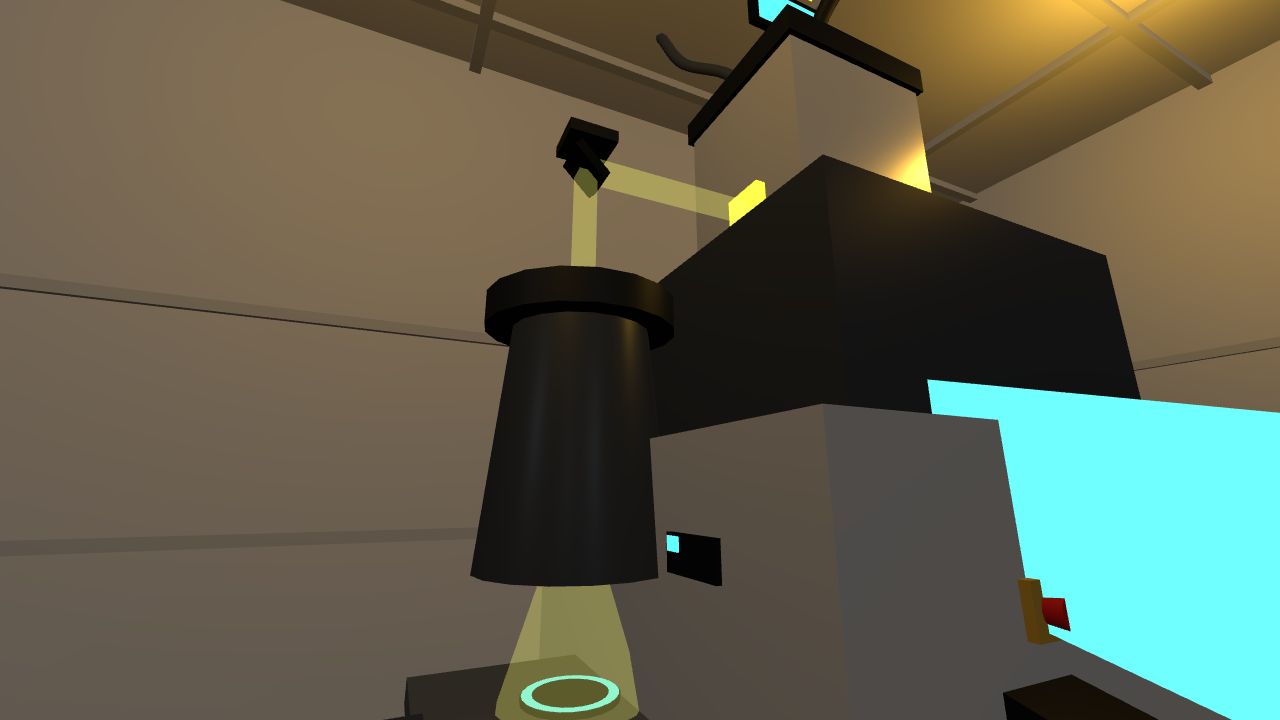
The amber partition fences off the yellow bay — photoresist is blind above 450 nm, so coat track, stepper and the ion implanter (resist is the implant mask) live under yellow light. The white bay holds RIE etch, the double-angle evaporator, the α-Ta sputter tool, a wet bench and CD-SEM metrology; probe, dicing and wire bonding sit in the test corner. Siting is a ledger item, not a mood: surface dust storms raise particle counts a thousandfold, while the cavern gives constant temperature and zero wind vibration.
The downflow itself is a number. At 0.35 m/s the piston flow sweeps the full 5.7 m room height in 16 seconds; a 0.5 µm particle left to settle under Mars gravity would need 11.5 days. A factor of ~61,000 — cleanliness comes from the flow field, not from falling.
A 104-second choreography, written as a pure function of time — jump in at any moment and the state is self-consistent.
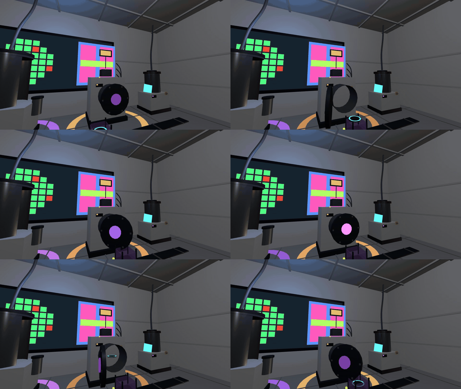
An AGV carries the hero wafer (cyan edge ring) from its charging dock to the coat track; a SCARA rail robot hands it between track and stepper; the AGV then crosses the fab to the RIE — whose chamber door swings open for it — then serves probe station and dicing saw before returning empty. Causality is enforced, not decorated: the exposure beam fires only while the wafer sits on the stage, the plasma ignites only after the chamber door seals, and the wafer map repaints die by die only while the probes are down. After each exposure a reticle handler swaps in the next layer's mask; every 11th lap is a reject lot whose edge ring turns red at the probe verdict.
Every product of this fab ships to another district of the same city — the supply chain closes inside the map.
A character-level bigram language model in silicon, RTL→GDS on an open toolchain, racked in the compute center.
Pixel front-ends and array mux for the city's single-photon sensors — the heaviest verification ledger on any line.
Dolan double-angle evaporation for the quantum center's 20-qubit chip — the stage in the scene rocks to the real ±28.6°.
Where a card claimed a mechanism, we ran the calculation — eighteen rounds of it, from partially-coherent imaging on the stepper down to the plasma inside the etcher and the alumina barrier in the evaporator, every number behind a known-answer gate.
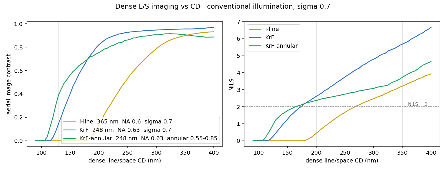
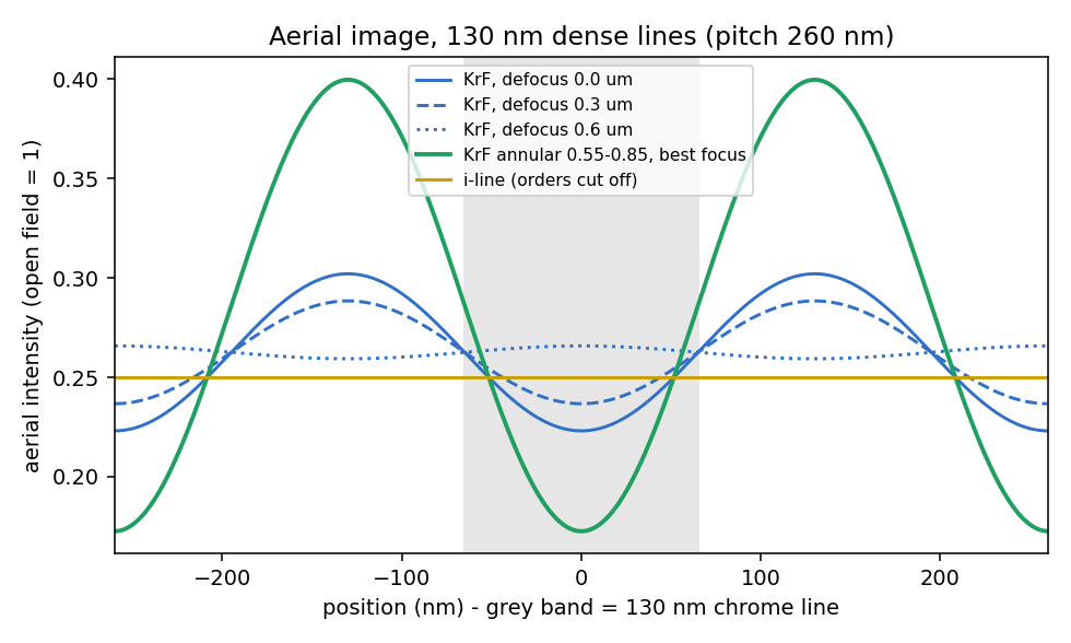
Printing 130 nm is not free. The Abbe simulation says i-line 365 nm passes zero diffraction orders at 130 nm dense pitch (cutoff 358 nm — contrast is exactly 0), and even KrF 248 nm with conventional illumination manages only 0.15 contrast at k₁ = 0.33. What rescues the node is annular off-axis illumination: two-beam imaging at contrast 0.40, NILS 1.25, with aerial depth-of-focus pushed beyond ±2 µm. "i-line for non-critical layers, KrF plus off-axis for critical ones" is diffraction physics, not a cost choice.
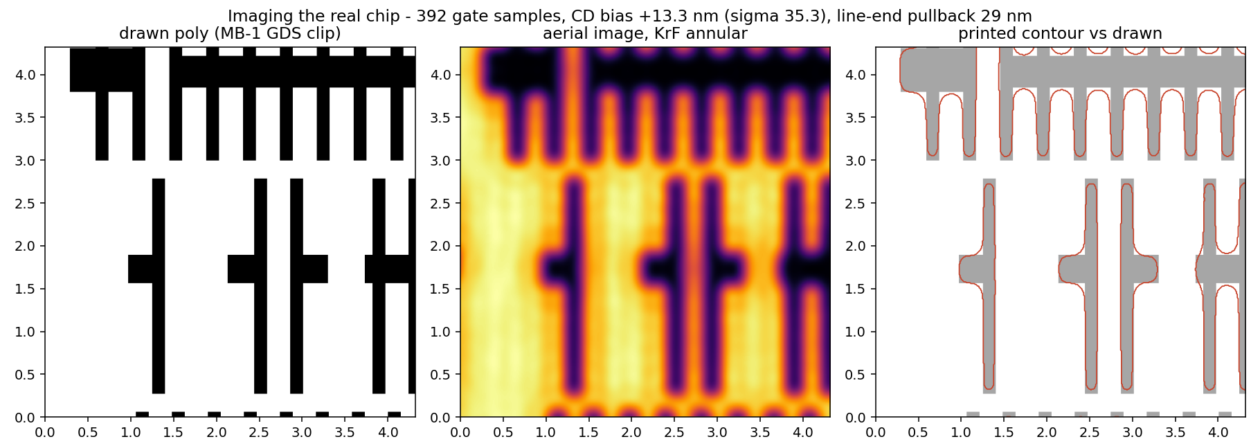
Round two imaged the actual chip. A 6% attenuated phase-shift mask lifts NILS from 1.25 to 1.69 and exposure latitude from 11% to 15% — but MEEF at k₁ = 0.33 is 2.79, so every mask CD error lands on the wafer nearly tripled. Then a 5 × 5 µm clip of MB-1's signed-off poly GDS went straight through the same imaging model: across 392 real gate samples, single-dose printing with no OPC leaves a +13 nm mean bias with a 35 nm (1σ) proximity spread, pulls line ends back by 29 nm (p95: 90 nm), and drops a few slivers entirely — while bridging nothing. OPC and phase-shift masks are not polish; they are the steps that cancel exactly these entries.
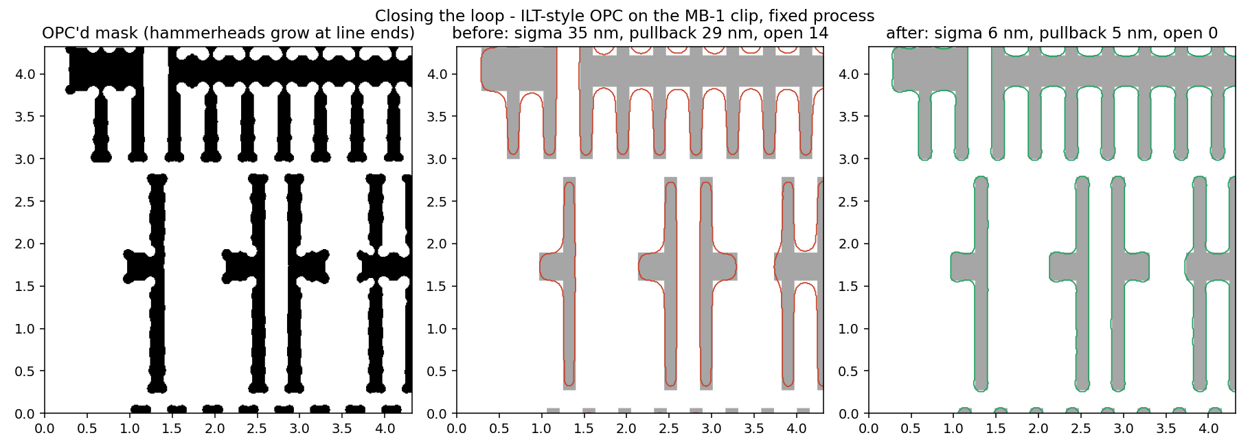
Round three closed the loop. With the process locked — same annular source, same dose calibration — twelve ILT-style pixel iterations corrected only the mask: CD spread fell from 35 to 5.9 nm, line-end pullback from 29 to 4.6 nm, and all fourteen lost slivers came back. The best part is in the corrected mask itself: hammerheads grew at the line ends on their own. Nobody wrote that rule — it is the imaging physics' own solution to cancelling pullback, rediscovered by the loop.
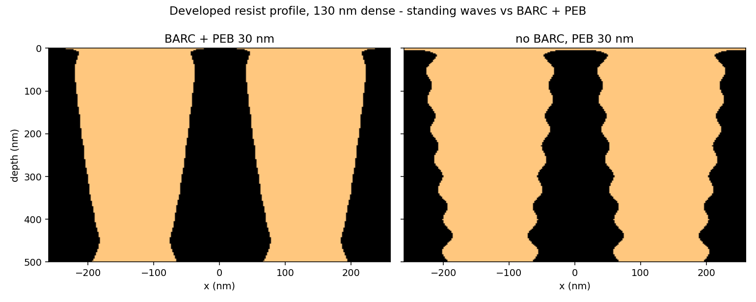
Round four pushed the light into the resist. Silicon reflects 53% at 248 nm, printing 70 nm-period standing waves into the film; a transfer-matrix scan lands the anti-reflective coating at 108 nm, crushing residual reflectivity to 0.5% and the dose-vs-thickness swing from 0.48 to 0.06. A Dill-exposure / acid-diffusion / Mack-development chain then grows the actual resist profile: 84.6° sidewalls with 1.4 nm edge ripple under BARC and a 30 nm bake diffusion — strip the BARC and the same recipe pays 14% more dose while the sidewalls scallop at triple the ripple.
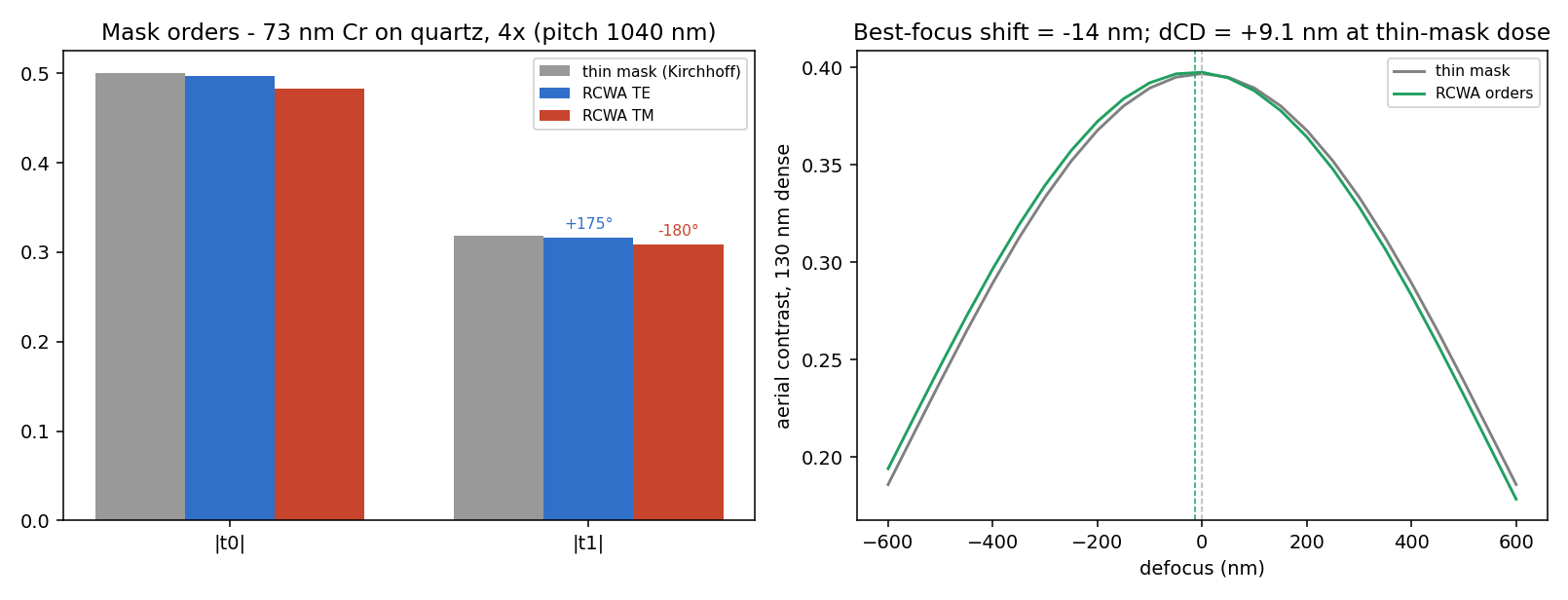
Round five put the mask itself on trial. Every round above treated the reticle as an infinitely thin transmission function — but a real 4× mask is 73 nm of chrome standing on quartz. An in-house RCWA solver (the rigorous-coupled-wave engine behind commercial mask-3D tools, validated to machine precision against Fresnel and to 1.0 in energy conservation) diffracted the real stack: order amplitudes land within 3.4% of the thin mask, phases within 5°, and at the wafer that prices out to a −14 nm best-focus shift plus a 1.4% dose error. Verdict: Kirchhoff holds at 130 nm / 4× — the foundation under every result above is sound, and mask 3D becomes a first-class citizen only at high-NA and EUV.
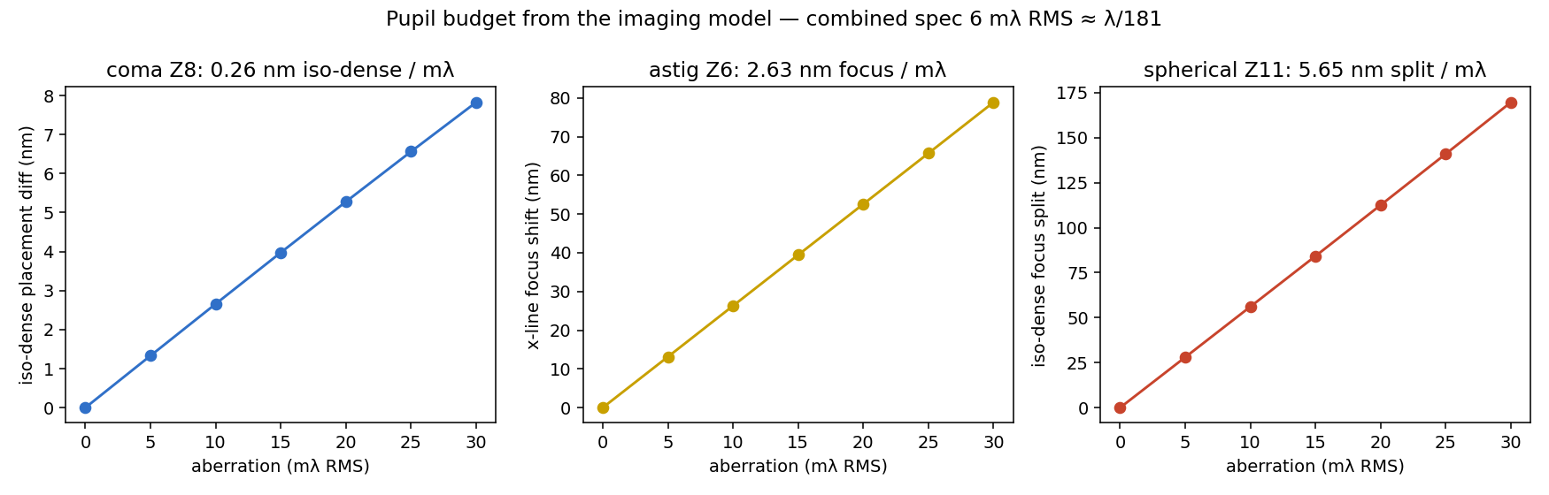
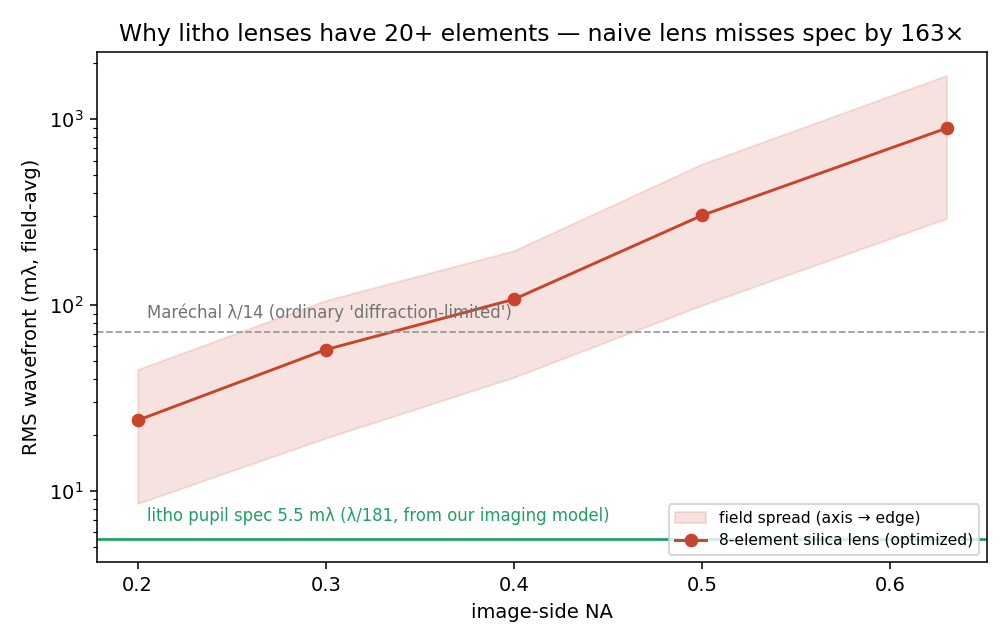
Round six specified the lens — and then measured one. Injecting Zernike aberrations into the imaging pupil prices each milliwave at the wafer (with a lesson en route: dense lines are immune to coma shift, so the honest coma metric is iso-dense placement). The budget lands at coma 7.7, astigmatism 19, spherical 8.8 mλ — 5.5 mλ RMS combined, ≈ λ/181, thirteen times tighter than the usual "diffraction-limited" λ/14. Zemax OpticStudio, driven headless through the ZOS-API, then optimized a naive 8-element all-silica 4× objective to convergence: at NA 0.63 it reaches 896 mλ — 163× off spec. That gap is the entire reason real DUV objectives are twenty-plus-element, ten-million-dollar monsters.
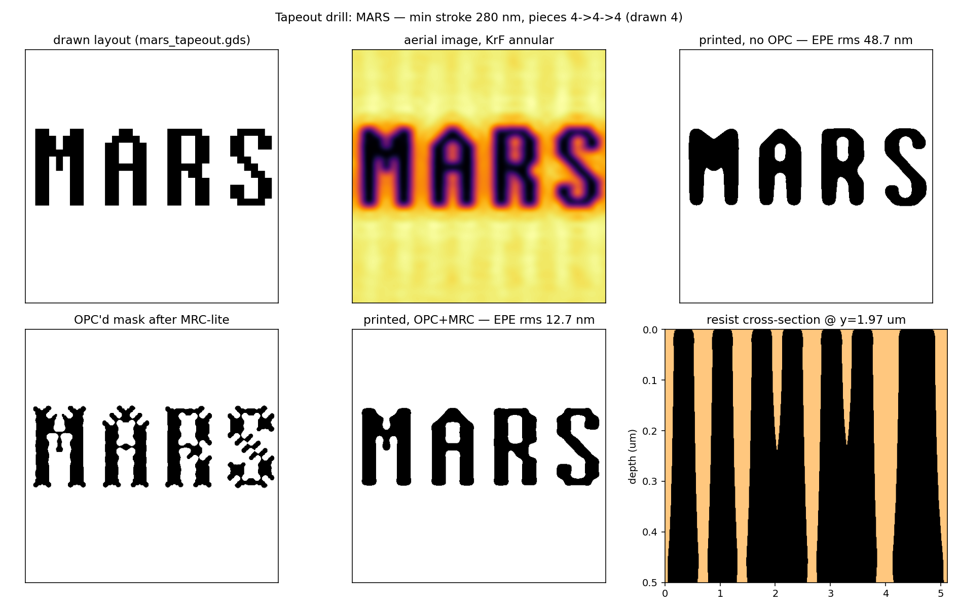
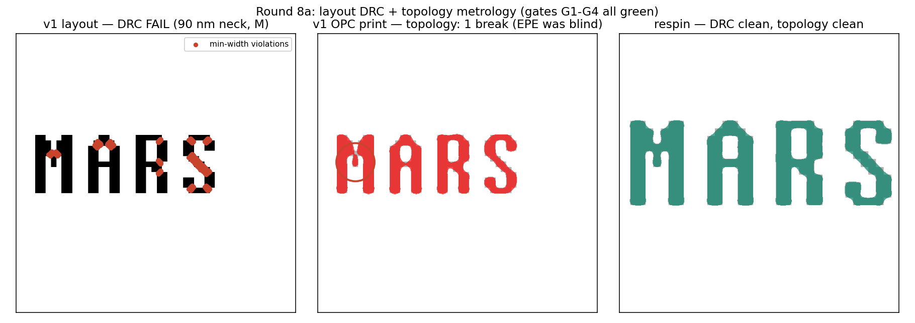
And then the line ran a real job. A dry-run tapeout pushed the word MARS — an actual GDS, drawn in a polygon font — through the whole flow: mask, annular imaging, dose-to-size, OPC, resist. First silicon failed honestly: the font carried a 90 nm neck in the M (half the process minimum), the printed letter broke in two — and the EPE metric never noticed (12.4 nm, unchanged); only a topology count caught it. A DRC-driven respin at 280 nm strokes printed all four letters clean at EPE 12.7 nm. The drill's real product is its gap list: layout DRC, topology-aware metrology, mask rule checks, 3D resist, etch transfer — the next roadmap, discovered by taping out.
Then the drill's gap list got worked off. A layout DRC now exists (minimum width by erosion-split — the naive morphological opening false-flags every right-angle corner; learned the hard way), and run against the v1 layout it flags twenty sub-130 nm junctions — the print had broken exactly at the worst one. A topology metrology (breaks / bridges / missing) catches what EPE cannot, locating the M break precisely. And an anisotropic etch-front model carries the resist profile into the film through three limit gates: ideal RIE inherits the resist's footprint (154 = 154 nm, 90° walls), isotropic undercut matches film depth (295 ≈ 300 nm), and selectivity bookkeeping closes (128 ≈ 130 nm). Production point: the 130 nm resist line lands in the film at 138 nm, 90° sidewalls, with 372 nm of resist to spare. The word is in the film now.
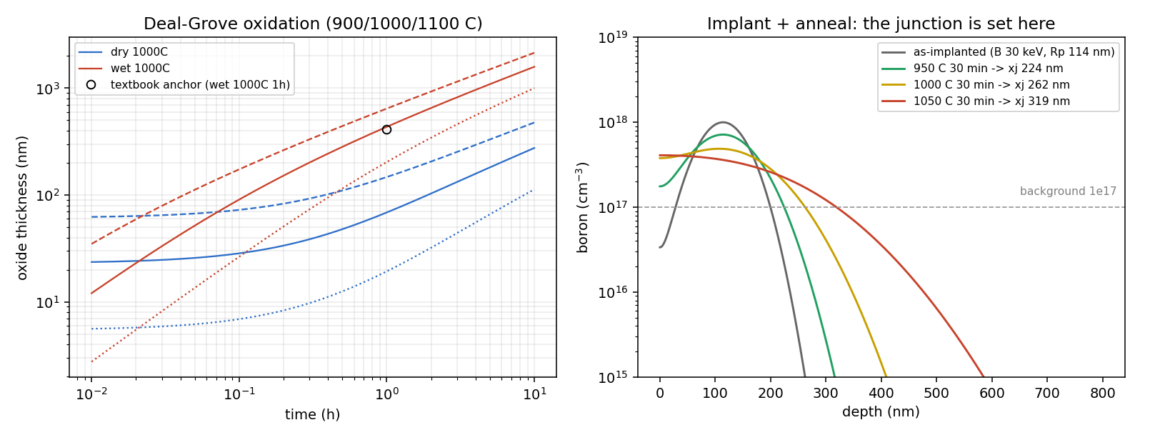
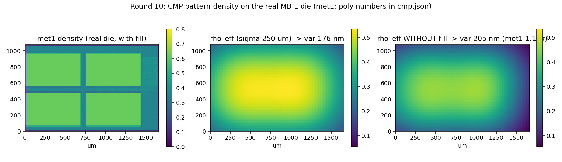
Two more unit processes joined the ledger. Thermal: Deal-Grove oxidation gated on its own asymptotics and a textbook anchor (wet 1000 °C/1 h: 435 vs ~410 nm), and the round-2 implant profile annealed into real junctions — 224 / 262 / 319 nm at 950/1000/1050 °C — after the dose-conservation gate caught a plain Gaussian leaking up to 21% of the implant out of the wafer (the surface needs a reflecting boundary). CMP: a Stine pattern-density model over the real MB-1 metal-1 density map puts within-die post-polish variation at 176 nm — comfortable against this node's >±2 µm depth of focus. And the fill-cell counterfactual dissected a slogan: metal-1 owes its uniformity to the power grid, while on poly the 54k decap cells lift the emptiest density bins tenfold — fill is first about uniformity; CMP is only one of its motives.
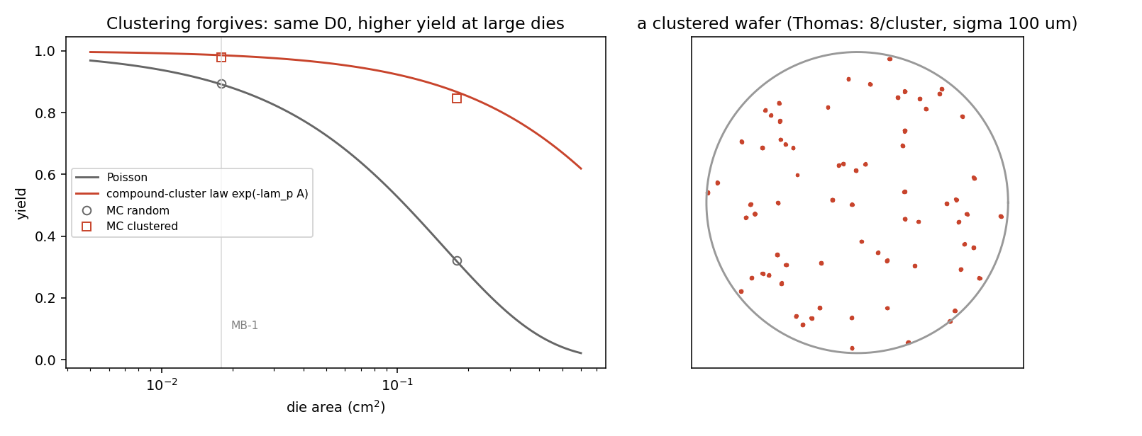
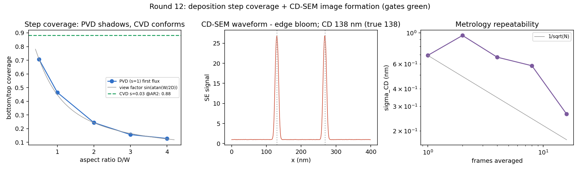
The last ledger pages: statistics, deposition, metrology. Yield beyond Poisson: at the same D₀ = 6.4/cm², defects arriving eight to a cluster lift a hypothetical 10× die from 31.8% to 84.7% — clustering is merciful — and the Monte Carlo taught its own lesson: the statistical family follows the clustering mechanism (compound clusters give a rescaled Poisson; regional variation gives the negative binomial; force-fitting NB yields a scale-drifting α). Deposition: line-of-sight sputtering leaves 24% coverage at the bottom of an AR-2 trench — exactly the view factor, 0.244 vs 0.243 — while the low-sticking CVD limit conforms at 0.88. And the CD-SEM got an image-formation model: edge bloom, 3 nm spot, shot noise, σ_CD 1.04 → 0.34 nm under 16-frame averaging, following 1/√N as metrology should.
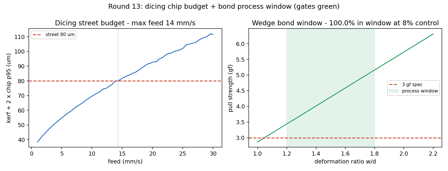
Then the back end closed its own books. Dicing got a chip-budget model: per-grit engagement δ = feed/(rpm × grits), backside chipping growing by the indentation-fracture scaling c ∝ δ^(2/3) — at 10 mm/s the chip p95 is 19.7 µm, so the 30 µm kerf plus both chip margins uses 69.4 µm of the 80 µm street, with 14.3 mm/s as the ceiling. Wire bonding got a process window: the 25 µm Al wedge deformation ratio lands in r ∈ [1.2, 1.8], 4.3 gf of pull at center — above the 3 gf spec, below the 7.5 gf wire break — and a unit-slip lesson: a stray ×1000 briefly gave the wire a 7,505 gf "break strength", which is exactly why the sanity gate carries an upper bound.
Then an audit went looking for the tools whose performance outran their paperwork. Mapping every tool against every sub-component turned up four places where the scene showed a mechanism convincingly and the ledger held nothing at all: the wet bench, the coater's film thickness, the plasma inside the etcher, and the tunnel barrier grown in the evaporator's oxygen glow. Four rounds closed them.
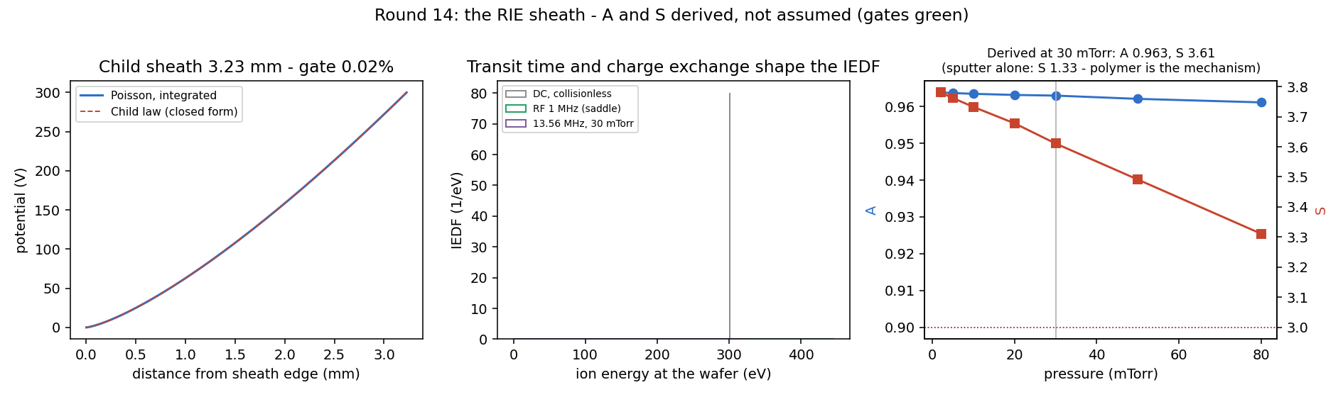
The etcher got its plasma. Rounds up to here took anisotropy A = 0.9 and selectivity S = 3 as inputs — the deepest etch result in the project resting on two hand-picked numbers. Integrating Poisson's equation for the sheath (3.2275 mm against the Child law's 3.2281) and pushing Monte-Carlo ions across it, with charge exchange happening 1.17 times per crossing, produces an ion angular distribution that fixes A = 0.963 with no free parameter at all. Selectivity refused the same treatment: sputter yields alone give 1.33, nowhere near what fluorocarbon etching really delivers, because selectivity is not a yield ratio — it is the polymer passivation layer, held thinner on oxide (1.5 nm) than on resist (3.0 nm) because the oxide releases its own oxygen. Feeding the derived pair back moved the film CD from 138 to 150 nm: the old assumption was 12 nm pessimistic.
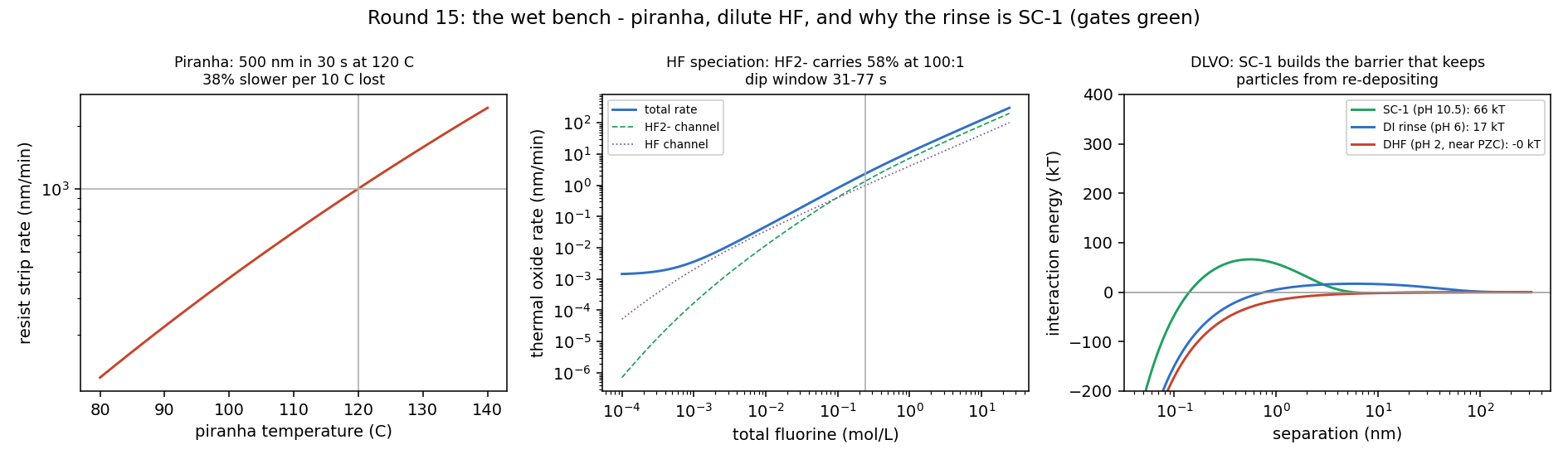
The wet bench got three ledgers, and one of them is a warning. Piranha strips the 500 nm resist in 30 s at 120 °C and loses 38% of its rate for every 10 °C the tank sags. Solving the HF ionisation and dimerisation equilibria shows HF₂⁻ carrying 58% of the etch rate and sets a dip window of 31–77 s, with native oxide regrowing to half a nanometre in 0.45 h — that is the queue-time limit. And the DLVO calculation explains why an HF step is always followed by a rinse: SC-1 raises a 66 kT barrier that keeps particles off the wafer, while the HF tank itself, sitting at pH 2 near silica's point of zero charge, offers −0.1 kT and lets them re-deposit.
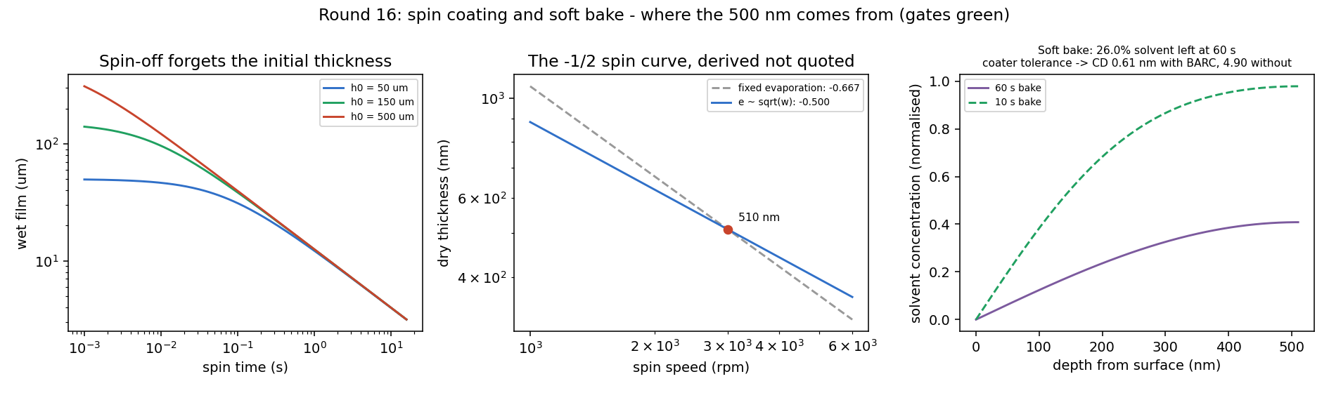
The coater's 500 nm became a result. Spin-off famously makes the film forget its initial thickness — 50 µm and 500 µm starts converge to 0.05% — and the Meyerhofer criterion sets it where thinning falls below evaporation. That gives ω^(−2/3), yet every spin curve ever measured shows −1/2; the missing piece is that evaporation itself follows √ω through the rotating-disk boundary layer, and restoring it yields exactly −0.500. At 3000 rpm the film lands at 510 nm. The tolerance then propagates: ±0.5% on spin speed becomes 4.9 nm of CD error without BARC and 0.61 nm with it, so the coater's precision spec is really the anti-reflective layer's decision.
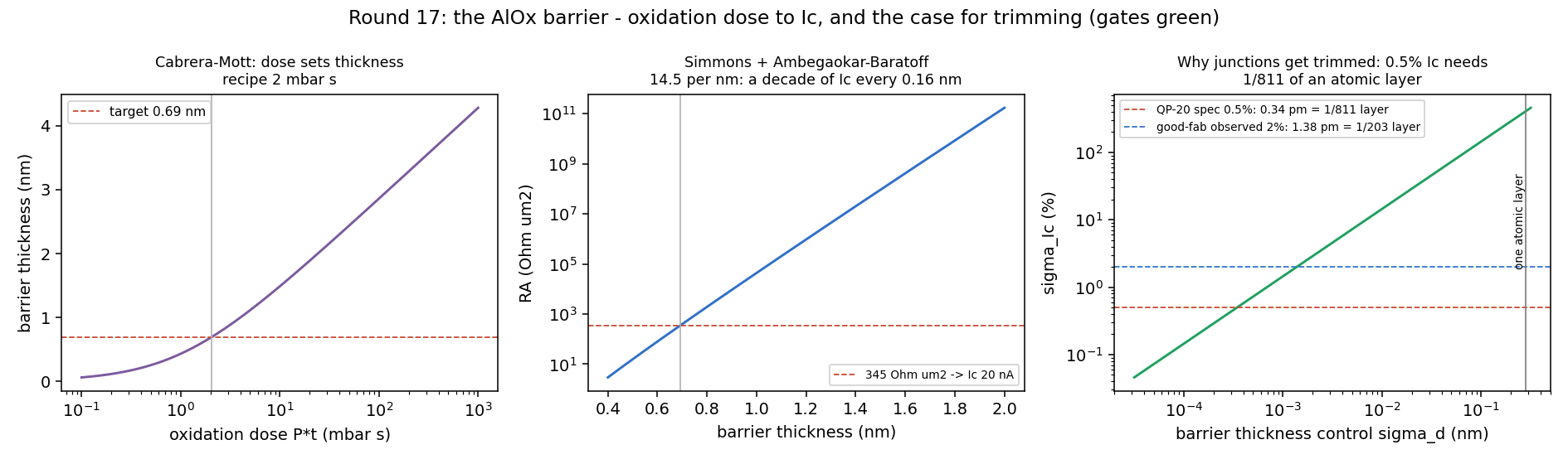
And the barrier explained why junctions get trimmed — again. Oxidation dose to thickness to tunnel resistance to critical current, with IcRn landing at 282.7 µV against the known 283, inverts a 10 GHz EJ to a barrier just 0.691 nm thick. Tunnelling then punishes every picometre: holding Ic to 0.5% requires thickness control of 0.345 pm, one 811th of an atomic layer. Pointwise that is impossible, and junctions only work because roughly 4×10⁴ independent atomic patches average the barrier down to the few percent good fabs actually see. Round 2 reached "trimming is mandatory" from evaporation tilt; this reaches it from barrier thickness. Two unrelated routes, one process decision.
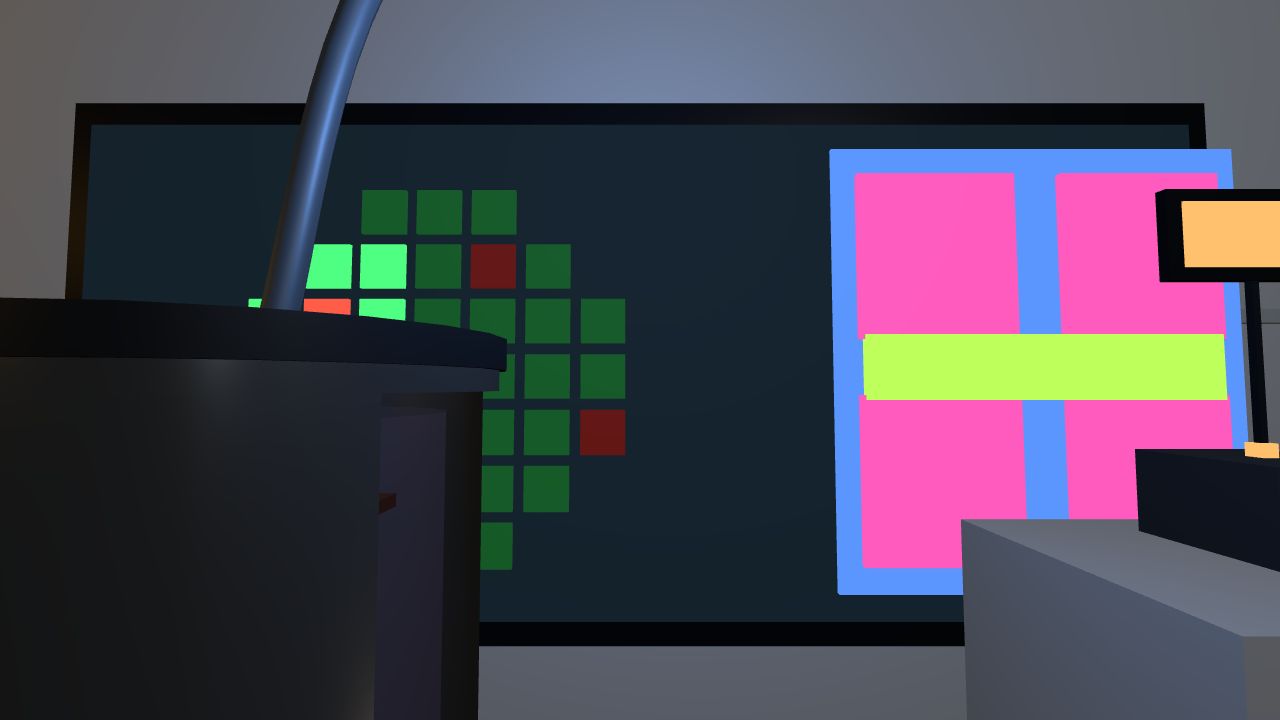
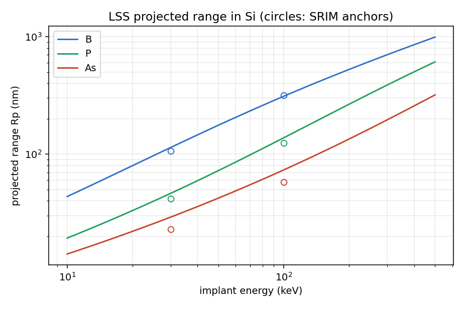
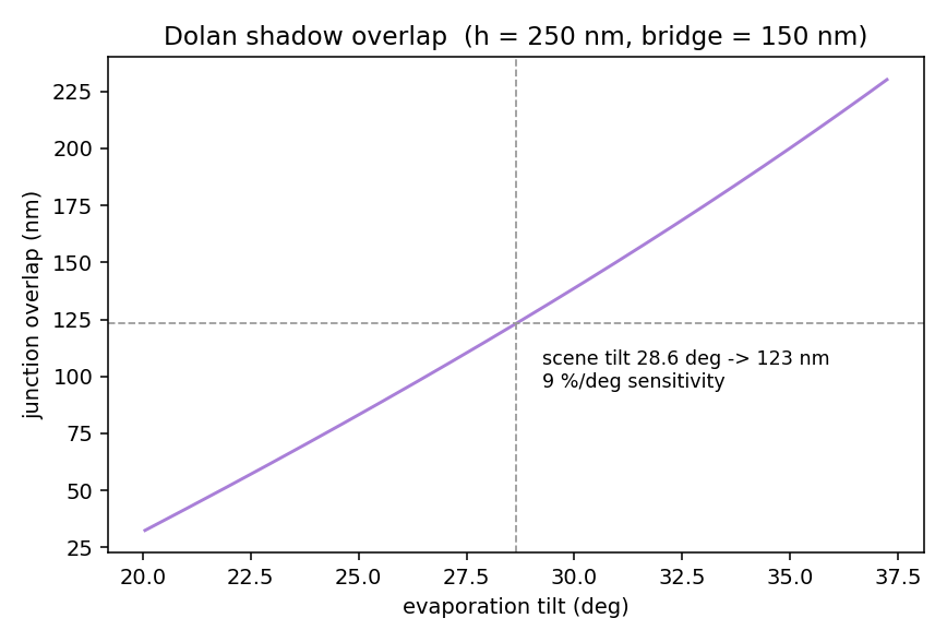
And the other machines got their numbers too. First-order LSS ranges put boron at ~114 nm for 30 keV and ~311 nm for 100 keV (checked against SRIM anchors: B/P within 11%, As reads +27% high — a declared bias of the first-order model). The Dolan shadow geometry, evaluated at the scene's own tilt, shows why junction trimming exists at all: holding a 0.5% area spread by geometry would need the tilt repeatable to 0.054°. And the wall screen's wafer map inverts, through a Poisson model, to a defect density of 6.4 /cm² — at which a die ten times MB-1's size would yield only 32%.
Every number on this page, and the run that produced it.
| Claim | Value | Produced by |
|---|---|---|
| i-line cutoff, dense pitch | 358 nm (contrast = 0 below) | mars-fab/sim/litho_aerial.py |
| KrF conventional @ 130 nm | contrast 0.15, k₁ = 0.33 | mars-fab/sim/litho_aerial.py |
| KrF annular 0.55–0.85 @ 130 nm | contrast 0.40, NILS 1.25 | mars-fab/sim/litho_aerial.py |
| Aerial DoF, ±10% CD | > ±2 µm | mars-fab/sim/litho_aerial.py |
| att-PSM gain @ 130 nm | NILS 1.25 → 1.69, EL 11 → 15% | mars-fab/sim/litho_process.py |
| Mask error enhancement (MEEF) | 2.79 @ 130 nm | mars-fab/sim/litho_process.py |
| Real-GDS gate CD spread, no OPC | +13 nm mean, σ 35 nm (392 gates) | mars-fab/sim/litho_gds2d.py |
| Line-end pullback on MB-1 poly | 29 nm mean, p95 90 nm | mars-fab/sim/litho_gds2d.py |
| Post-OPC gate CD spread | σ 5.9 nm (12 iterations) | mars-fab/sim/litho_opc.py |
| Post-OPC pullback / defects | 4.6 nm · opens 14 → 0 | mars-fab/sim/litho_opc.py |
| Standing waves / BARC design | Si R 53% → 0.5% @ 108 nm | mars-fab/sim/litho_resist.py |
| Resist profile (BARC + PEB) | 84.6° sidewall, 1.4 nm ripple | mars-fab/sim/litho_resist.py |
| Cost of skipping BARC | +14% dose, 3× scallop ripple | mars-fab/sim/litho_resist.py |
| Mask-3D order error (73 nm Cr, RCWA) | ≤3.4% amp, ≤5° phase | mars-fab/sim/litho_mask3d.py |
| Kirchhoff verdict at wafer | −14 nm focus shift, 1.4% dose | mars-fab/sim/litho_mask3d.py |
| Pupil aberration spec (derived) | 5.5 mλ RMS ≈ λ/181 | mars-fab/sim/litho_pupil_budget.py |
| Naive 8-element lens @ NA 0.63 | 896 mλ — 163× off spec | mars-fab/sim/litho_lens_zemax.py (ZOS-API) |
| Coma metric lesson | dense lines immune; iso-dense 0.26 nm/mλ | mars-fab/sim/litho_pupil_budget.py |
| Tapeout drill: MARS, first silicon | M broke at a 90 nm neck; EPE blind to it | mars-fab/sim/tapeout_mars.py |
| Tapeout drill: DRC respin | 4/4 letters, EPE 12.7 nm | mars-fab/sim/tapeout_mars.py |
| Layout DRC on v1 (min width 130 nm) | 20 violations; print broke at worst | mars-fab/sim/litho_drc.py |
| Etch transfer, 3 limit gates | 154=154 · 295≈300 · 128≈130 nm | mars-fab/sim/litho_etch.py |
| MARS line in the film (RIE A=0.9, S=3) | 138 nm CD, 90° sidewall | mars-fab/sim/litho_etch.py |
| Junction depths, B 30 keV + 30 min anneal | 224/262/319 nm @ 950/1000/1050 °C | mars-fab/sim/proc_thermal.py |
| Dose-conservation gate catch | plain Gaussian leaks up to 21% | mars-fab/sim/proc_thermal.py |
| Post-CMP spread, real MB-1 met1 | 176 nm (ρ_eff 0.18–0.53) | mars-fab/sim/proc_cmp.py |
| Fill counterfactual on poly | decap lifts min density 10× | mars-fab/sim/proc_cmp.py |
| Clustering bonus at a 10× die | 31.8% → 84.7% (+52.9 pp) | mars-fab/sim/proc_yield.py |
| Trench bottom coverage = view factor | 0.244 vs 0.243 (AR 2, PVD) | mars-fab/sim/proc_dep_sem.py |
| CD-SEM repeatability | σ 1.04 → 0.34 nm @ 16 frames | mars-fab/sim/proc_dep_sem.py |
| Dicing street budget (chip p95 19.7 µm) | 69.4 / 80 µm; max feed 14.3 mm/s | mars-fab/sim/proc_dice_bond.py |
| Wedge bond window, 25 µm Al | r 1.2–1.8 · 4.3 gf > 3 gf spec | mars-fab/sim/proc_dice_bond.py |
| Implant ranges B/P/As vs SRIM | B/P ±11%, As +27% | mars-fab/sim/fab_calcs.py |
| Dolan overlap & tilt sensitivity | 123 nm · 9.2%/deg | mars-fab/sim/fab_calcs.py |
| Defect density from wafer map | D₀ = 6.4 /cm²; 10× die → Y 32% | mars-fab/sim/fab_calcs.py |
| Downflow sweep vs settling | 16 s vs 11.5 days | mars-fab/sim/fab_calcs.py |
| MB-1 dual-simulator lockstep | 1,134,185 ns bit-exact | mars-bigram (iverilog + xsim) |
| MB-1 FPGA prototype timing | WNS +3.29 ns | mars-bigram (Vivado, Arty A7) |
| SRAM macro equivalence | 11,069 reads, 0 mismatch | mars-bigram (OpenRAM TB) |
| MB-1 final GDS | 26.3 MB, routing DRC 0 | mars-bigram (OpenROAD + klayout) |
| Analog DRC convergence | ~29 rounds; arr4 51 → 0 | mars_spad_rox (Calibre DRC) |
| Analog LVS / PEX / post-layout | 11× CORRECT / 3 / 4 | mars_spad_rox (Calibre, xRC, Spectre) |
| Analog Monte-Carlo trip points | 40 | mars_spad_rox (Spectre MC) |
| JJ yield vs σEJ | 99.6% @ 0.5%; collapse @ 1% | quantum-computing/sim (freq-collision MC) |
| QP-20 layout v7 | 2,367 polygons, DRC-lite 0 | quantum-computing (gdstk, 7 rounds) |
| Bond-out feasibility | 87 pads, 0 violations | quantum-computing/sim (bonding DRC) |
| Sheath: Poisson integration vs Child law | 3.2275 vs 3.2281 mm (0.02%) | mars-fab/sim/proc_plasma.py |
| Etch anisotropy, derived not assumed | A = 0.963 (film CD 138 → 150 nm) | mars-fab/sim/proc_plasma.py |
| Selectivity without polymer passivation | S = 1.33 vs 3.61 with | mars-fab/sim/proc_plasma.py |
| Piranha strip, and its temperature cliff | 500 nm in 30 s; −38% per 10 °C | mars-fab/sim/proc_wetclean.py |
| Dilute-HF dip window | 31–77 s; HF₂⁻ carries 58% | mars-fab/sim/proc_wetclean.py |
| DLVO barrier, SC-1 vs the HF tank | 66 kT vs −0.1 kT (re-deposition) | mars-fab/sim/proc_wetclean.py |
| Spin curve exponent, derived | −0.500 once e ∝ √ω; 510 nm at 3000 rpm | mars-fab/sim/proc_coat.py |
| Coater tolerance → CD | 4.9 nm without BARC, 0.61 nm with | mars-fab/sim/proc_coat.py |
| AlOx barrier for a 10 GHz EJ | 0.691 nm; IcRn 282.7 vs 283 µV | mars-fab/sim/proc_alox.py |
| Thickness control σIc = 0.5% demands | 0.345 pm = 1/811 of an atomic layer | mars-fab/sim/proc_alox.py |
| Scene choreography integrity | 520-frame envelope sweep, 0 console errors | viewer/units/ops-fab-01.js (headless CDP) |
The honest section. Everything below cost real hours.
Conventional illumination failed at 130 nm — a genuine surprise. The imaging study was expected to bless k₁ = 0.33 and instead returned contrast 0.15: at axial illumination most of the ±1st orders miss the pupil. Annular illumination wasn't an optimization, it was the difference between a fab and a sculpture. The first DoF sweep also saturated its own ±1 µm scan range; extending to ±2.5 µm showed two-beam imaging simply isn't focus-limited, and the page reports that honestly instead of quoting a fake edge.
TritonRoute refused constant nets (DRT-0305). The most-quoted of MB-1's six physical-design pitfalls: tie cells are not optional. The analog line's arr4 block opened at 51 DRC violations and took the bulk of 29 rounds to reach zero — a layout is not done when drawn; it is converged under the rule deck.
A wrong number density nearly shipped as an exciting discovery. The plasma round's first pass paired a resist number density counted per atom with a sputter yield defined per repeat unit — an order-of-magnitude mismatch. Out came S = 0.65, which says the mask clears before the film does, which says oxide etching is impossible. It read exactly like a real finding: a clean falsification with a tidy mechanism story attached. Nothing in the gate set caught it, because every gate was a ratio, and ratios are blind to a factor shared by numerator and denominator. What caught it was adding an absolute-rate anchor — film 30–60 nm/min, resist 15–40 — which the mistaken parameters missed by 10×. The lesson outlived the bug: a gate set made entirely of ratios and limits cannot see a unit slip, so at least one gate has to be pinned to an absolute magnitude.
Geometry can't hold σEJ. The Dolan calc puts tilt-error sensitivity at 9.2%/deg, so the 0.5% junction spread the yield MC demands would need 0.054° tilt repeatability. That number is why the trim step exists — discovered backwards, from a system simulation to a process spec.
The real-GDS round had traps of its own. The first "densest logic" window turned out to be 62% poly coverage — because 54,660 of MB-1's 68,234 placed cells are decap fill, and the density histogram had faithfully found a wall of capacitors. Logic-only filtering dropped it to a sane 27.7%. Then the CD metrology walked off a cliff: in dense regions the printed dark areas of neighbouring lines touch, and an unbounded edge-search returned 3-µm "gates" (σ = 556 nm). Bounding the search window and classifying merged/open features separately brought the statistics back to physics.
The resist model taught a lesson about credit. The no-BARC stack first refused to develop at any dose. One patch shipped two changes — moving the PEB blur from the protection field to the acid field, and calibrating dose-to-size per stack — and the fix was confidently attributed to the first. It wasn't. While building a reproducer for the skill distilled from this pipeline, the "bug" refused to reproduce: a Gaussian blur is linear and blur(1) = 1, so blurring m and blurring acid (= 1 − m) are mathematically identical. An ablation confirmed it — protection-field blur plus per-stack dose calibration reproduces every number to the digit. The real fix was the dose calibration (a reflective stack wastes dose in standing-wave nodes; borrowing the BARC recipe underexposes it). Attribution needs ablation: the passenger change in a two-change patch will happily take the driver's credit.
The RCWA solver briefly modelled a laser, not a mask. In the e−ikz convention a passive medium needs a negative imaginary index; chrome entered as 0.85 + 2.01j and became a gain medium, failing the uniform-layer Fresnel gate by 98% — while the energy-conservation gate, which only checks lossless gratings, passed obliviously. Two complementary validation gates, or the bug walks through.
The lens optimizer dove off a cliff once. Raising the magnification constraint's weight from 100 to 1000 made damped least squares tear the seed apart — magnification shot to +0.45, every ray failed to trace, and the merit function reported a flawless 0.0 over a lens that no longer worked. Constraint weights are not seatbelts; the stable recipe was two-stage (converge at weight 100, then polish at 400). And the first budget attempt measured coma by dense-line shift — which is exactly zero, because symmetric illumination cancels it; the overlay killer is the iso-dense difference.
Scene engineering bit back too. The SCARA robot's original 1.10 m reach could not touch both handoff stations; it was rebuilt at 1.05 m with keyframe-exact transfer points. Hidden browser tabs suspend requestAnimationFrame and produced false-dead animations during verification — all sign-off now runs through headless CDP with the choreography clock read directly. And the hero wafer once kept a stale position while invisible, breaking jump-in determinism; hidden segments now park it at a fixed pose.
Walk the line yourself — the fab is a live interior in the city viewer.
Open viewer/index.html?interior=ops-fab-01 (or enter through the undercity foyer). WASD to walk, walk into the exit ring or press Esc to leave. Get close to any tool for its bilingual knowledge card (EN toggle top-right); press V for the ring menu and fire the EMO stop demo — the whole choreography freezes under red alarm light and resumes without a time-jump. Capture tip: &fabT0=<seconds> shifts the choreography phase, so any beat of the 104 s lap can be reached on demand.
Things worth standing next to: the light pipe over the stepper (it only lights during exposure), the RIE door when the AGV arrives, the evaporator's rocking stage, and the wafer map while the probes are down.